

Ohio State holds ribbon-cutting for $20 million semiconductor research and prototyping expansion
New capabilities support industry partnerships and national defense technology development

The Ohio State University held a ribbon-cutting ceremony on Oct. 20 for a more than $20 million expansion of its semiconductor research and development infrastructure.
The new capabilities are designed to accelerate the transition of emerging semiconductor technologies from university laboratories toward defense and commercial manufacturing while supporting domestic workforce development and hands-on student training.
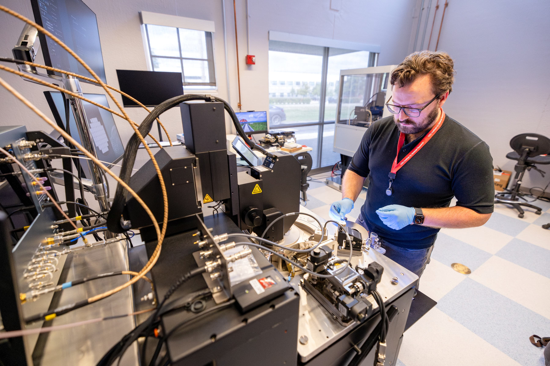
Operated by Ohio State’s Institute for Materials and Manufacturing Research (IMR), the Microelectronics Innovation and Technology Cluster (MITEC) connects and enhances existing facilities for semiconductor processing, device prototyping and testing.
“A defining responsibility of Ohio State’s land-grant mission is to generate new knowledge and share it with our students, giving them the opportunity to learn directly from groundbreaking discoveries,” said John M. Horack, vice president for research at Ohio State. “Just as important is our commitment to moving that knowledge beyond the laboratory, translating research into solutions that strengthen communities, improve lives and drive economic growth.”
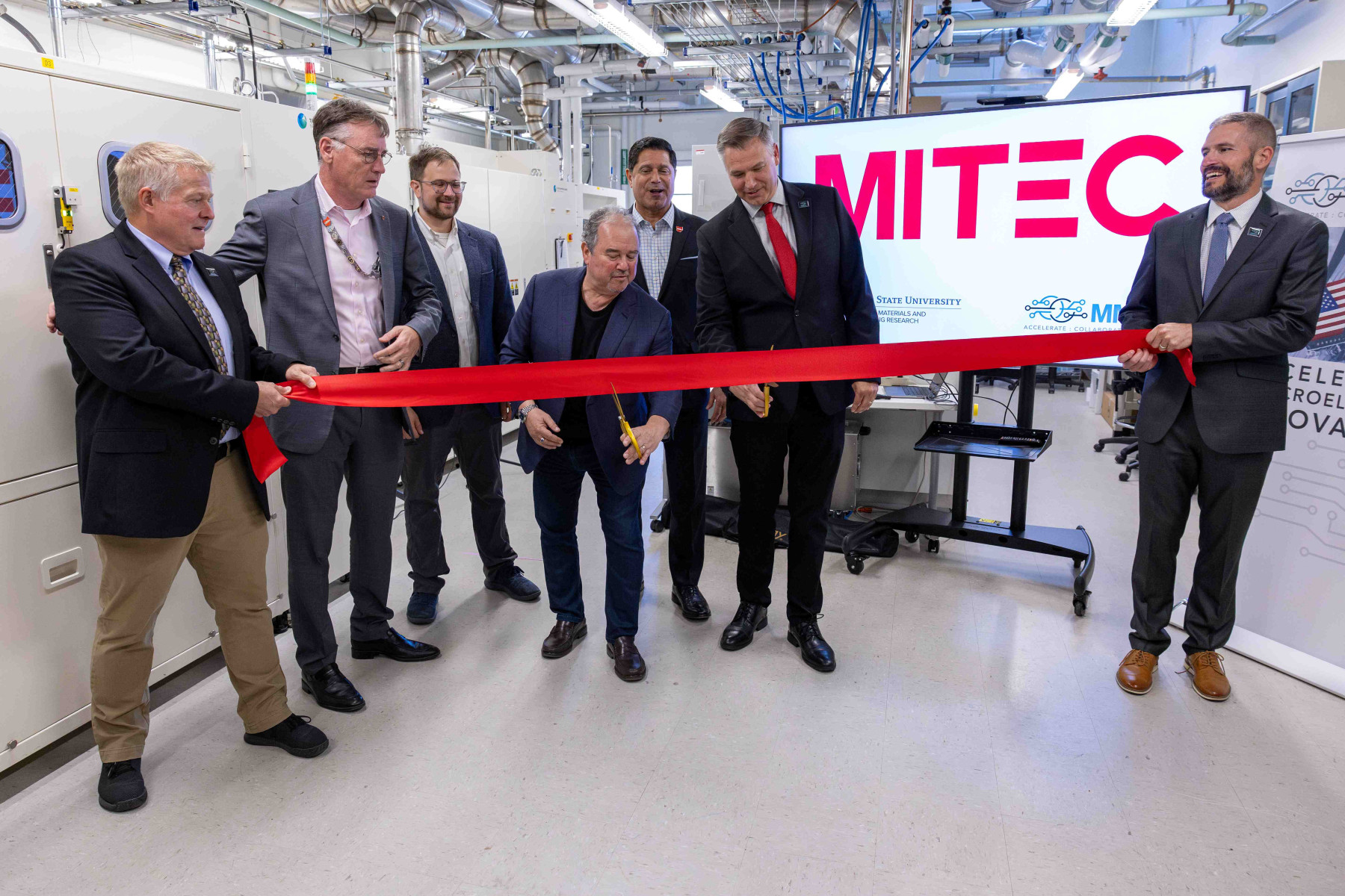 The expansion will support small and large industry partnerships and national defense technology development through the Midwest Microelectronics Consortium (MMEC), a Department of War-designated regional innovation hub.
“Ohio State is an important strategic partner and is aligned in MMEC’s mission to strengthen America’s microelectronics capabilities and supply chain,” said MMEC CEO Matt Casto. “MITEC represents more than an investment in infrastructure; it brings together world-class expertise, advanced facilities and industry partnerships to accelerate the development and transition of critical semiconductor technologies. By expanding access to these capabilities, we’re helping bridge the gap between research and real-world applications while strengthening the domestic microelectronics ecosystem.”
The initiative is supported by approximately $16 million in funding secured through MMEC, along with a roughly $4.5 million collaborative infrastructure investment from Ohio State and the Ohio Department of Higher Education.
These investments have funded major equipment additions and facility upgrades, expanding Ohio State’s ability to support university researchers and industry partners as they develop, evaluate and prepare state-of-the-art semiconductor technologies for manufacturing.
MITEC is led by Steven Ringel, a Distinguished University Professor and senior associate vice president for research at Ohio State.
“The new MITEC capabilities will have a significant impact on Ohio State’s semiconductor ecosystem and infrastructure, with the goal to support device development and prototyping for defense and commercial technology transitions working with the consortium,” Ringel said. “We are excited about our partnership with the MMEC as the Midwest’s leading innovation hub for compound semiconductor technologies.”
By bringing together these resources across Ohio State’s Nanotech West Lab and the Semiconductor Epitaxy and Analysis Laboratory, MITEC provides an integrated, flexible environment for collaborative technology development and rapid prototyping.
“It’s one thing to demonstrate something in a lab,” Horack said. “It’s another thing to do it at scale.”
MITEC supports semiconductor development using wafer sizes and processes compatible with industrial manufacturing beyond the expected scale of academic research. This allows researchers and industry partners to develop materials and prototype devices at a scale closer to commercial production, helping reduce the time needed to move new technologies from the laboratory into manufacturing and commercialization.
Workforce development and experiential learning initiatives are already underway, with MMEC-sponsored fellowships providing undergraduate and graduate students with hands-on research and prototyping experience in Nanotech West Lab’s cleanroom. Students work with wide bandgap semiconductors, materials used in high-power and high-speed electronics, as well as narrow bandgap semiconductors required for infrared sensing, while receiving training from experienced staff and helping accelerate the development of new technologies.
